


Scanning Electron Microscopy (SEM) Analytical Service
- Secondary Electrons (SE): Primarily used for imaging, providing detailed information about the surface topography and roughness of the sample.
- Backscattered Electrons (BSE): Sensitive to atomic number differences, offering compositional contrast between different materials.
- X-rays (EDS/EDX): Utilized for energy-dispersive spectroscopy, revealing elemental composition and spatial distribution.
- Limit the metal coating to 5–10 nm using ion sputtering or controlled thermal evaporation.
- Use low-voltage imaging (1–3 kV) to visualize moderately conductive regions without coating.
- For highly sensitive samples, opt for carbon coating or observe using field-emission SEM (FE-SEM) under low-current mode to capture the true surface morphology.
Scanning Electron Microscopy (SEM) Analytical Service is a high-resolution surface imaging and microstructural analysis service based on the interaction between a high-energy electron beam and the sample surface. It enables detailed observation of nanoscale to microscale surface features such as topography, particle morphology, fracture behavior, pore structure, texture alignment, and interlayer architecture.
In research fields such as materials science, biomedical engineering, nanotechnology, microstructural devices, and surface/interface science, understanding a material’s surface morphology, microstructure, and compositional distribution is fundamental to evaluating its functional performance. Structural characterization at the nanoscale can provide critical insights into the material’s physical properties, chemical reactivity, and biocompatibility. Conventional optical microscopy is limited by the wavelength of light and thus cannot meet the spatial resolution required for nanoscale analysis.
Scanning Electron Microscopy (SEM), as a high-resolution imaging tool for surface morphology and structural investigation, offers exceptional depth of field, magnification, and image clarity. It is suitable for the microstructural analysis of a wide range of materials, including conductors, semiconductors, insulators, and biological specimens.
MtoZ Biolabs provides Scanning Electron Microscopy (SEM) Analytical Service for a wide array of materials—including biological specimens, metals, polymers, composites, particles, and thin films. Our service supports microscopic morphology observation, dimensional measurement, cross-sectional analysis, surface structure characterization, etc.
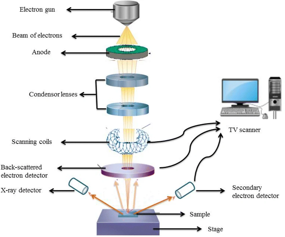
Technical Principles
Munir N. et al. Environ Sci Pollut Res. 2021.
The imaging principle of SEM is based on the interaction between a high-energy electron beam and the surface of the sample. As the focused electron beam scans across the sample surface, it generates multiple types of signals, including:
Signal generation and detection are synchronized with the scanning of the electron beam. These signals are converted into image data by an electron multiplier, ultimately producing high-resolution black-and-white topographic images or elemental mapping images. SEM enables detailed observation from the nanometer to micrometer scale, featuring high depth of field, wide field of view, and strong morphological contrast capabilities.
Analysis Workflow
MtoZ Biolabs' Scanning Electron Microscopy (SEM) Analytical Service covers the analytical process from sample preparation to data interpretation:
1. Sample Preparation
Samples are pretreated based on their nature. Biological or non-conductive materials are coated with a thin conductive layer (e.g., Au or Pt) or carbon. Volatile or soft materials may undergo cryo-fixation or vacuum drying to preserve structural integrity.
2. Instrument Parameter Configuration
Selection of appropriate accelerating voltage, working distance, and magnification.
Adjustment of secondary or backscattered electron detectors based on the material's characteristics.
3. Image Acquisition and Data Processing
Real-time tuning of focus, brightness, contrast, and other imaging parameters.
Capture of images from multiple angles and magnifications for key regions of interest.
4. Report Output
Delivery of high-resolution images.
Includes annotated images, dimensional measurements, and structural analysis explanations.
Applications
Scanning Electron Microscopy (SEM) Analytical Service supports microstructural research and material analysis across a broad range of disciplines, including:
Materials Science and Engineering
Analysis of surface morphology, particle size, and grain boundaries in metals, ceramics, and polymers.
Fractography, corrosion behavior, and interface structure characterization.
Electronics and Semiconductor Devices
Evaluation of thin film uniformity, micro/nano pattern structures, and defect detection.
Analysis of interlayer chip structures, contact interfaces, and packaging layers.
Biological and Medical Materials
Imaging of tissue sections, cellular structures, and membrane surface features.
Porosity and surface morphology analysis of biomaterials such as hydrogels and scaffolds.
Powder and Particle Analysis
Particle size distribution, surface roughness, and agglomeration behavior.
Morphological and dispersion analysis of pharmaceutical powders, catalysts, and nanoparticles.
Surface Treatments and Functional Coating Verification
Assessment of coating uniformity and adhesion failure analysis.
Observation of microstructural changes after surface etching, polishing, or plasma treatment.
FAQ
Q. Does the Thickness of Gold Coating on Non-Conductive or Biological Samples Affect Resolution and Surface Detail?
Yes, while gold coating improves conductivity and prevents charge accumulation—thereby stabilizing imaging—it can obscure nanoscale surface features if the layer is too thick, especially on soft materials.
Recommendations:
Q. Are Raw Images, Calibrated Measurement Data, and Image Analysis Reports Provided?
Yes. MtoZ Biolabs delivers a complete image data package, including high-resolution raw images (.tiff/.jpg), scale-calibrated annotated images, and publication-ready visual content. Upon request, we also offer quantitative image analysis services such as structural measurements, particle size analysis, and pore size statistics.
Case Study
This study utilized SEM to analyze the morphology of paramylon granules extracted from heterotrophically cultured Euglena gracilis. SEM imaging revealed that the extracted paramylon exhibited a highly crystalline particulate structure, closely resembling that of the analytical standard—thereby confirming the purity and structural integrity of the extract. Additionally, the study compared the effects of different extraction methods (e.g., SDS extraction and alkaline extraction) on paramylon morphology. Results indicated that extraction techniques influence both the surface characteristics and crystallinity of the granules.
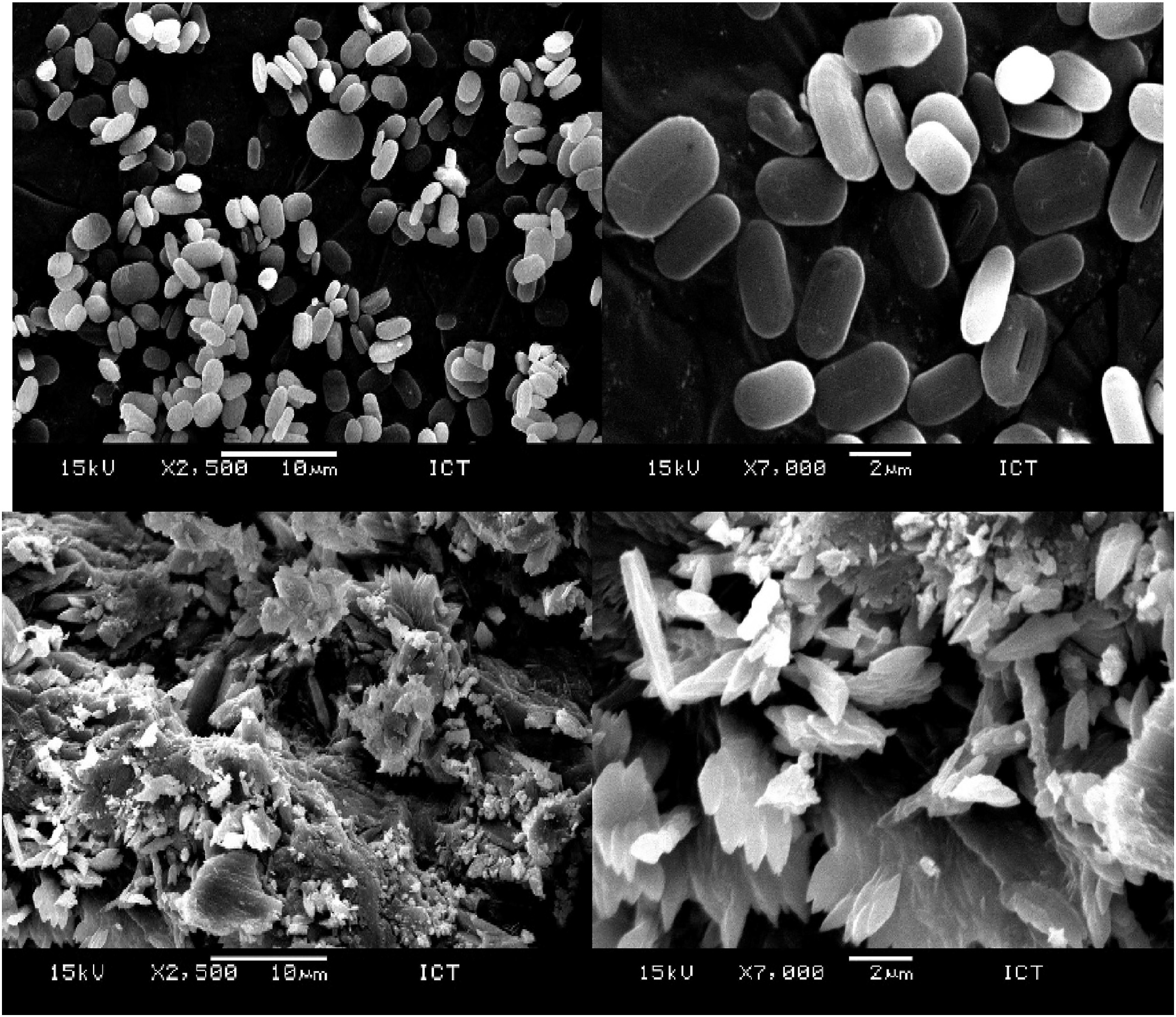
Bhattad T. et al. Heliyon. 2021.
MtoZ Biolabs, an integrated chromatography and mass spectrometry (MS) services provider.
Related Services
Structure&Component Analysis Services
Atomic Force Microscopy (AFM) Characterization Service
How to order?