


Aberration Corrected Scanning Transmission Electron Microscopy (AC-STEM) Analytical Service
Aberration Corrected Scanning Transmission Electron Microscopy (AC-STEM) is a state-of-the-art imaging and analytical technique that enables atomically resolved visualization and compositional analysis of materials at the sub-angstrom level. As a breakthrough in advanced electron microscopy, AC-STEM combines the scanning transmission electron microscopy (STEM) mode with sophisticated aberration correction systems, significantly enhancing spatial resolution and image clarity. This technology is indispensable for investigating atomic structures, chemical bonding, interface behavior, and defects in nanomaterials, semiconductors, catalysts, and functional thin films. In materials science, nanotechnology, and energy research, AC-STEM allows researchers to resolve individual atoms, quantify elemental composition, and correlate structure with function.
Technical Principles
Aberration corrected scanning transmission electron microscopy operates by focusing a finely converged electron probe onto the sample and raster-scanning it across the surface while detecting transmitted electrons. With the use of aberration correctors—usually correcting spherical and chromatic aberrations in the probe-forming lens—the system can achieve sub-angstrom resolution, allowing the direct observation of atomic columns.
Key modes include:
💠STEM-HAADF (High-Angle Annular Dark Field): Provides Z-contrast imaging where heavier elements appear brighter, offering direct insight into atomic column arrangements.
💠EDS Mapping (Energy-Dispersive X-ray Spectroscopy): Collects characteristic X-rays to map elemental distributions across nanoscale regions.
💠EELS Mapping (Electron Energy Loss Spectroscopy): Measures energy losses of inelastically scattered electrons to determine electronic structure, chemical bonding states, and light element distributions.
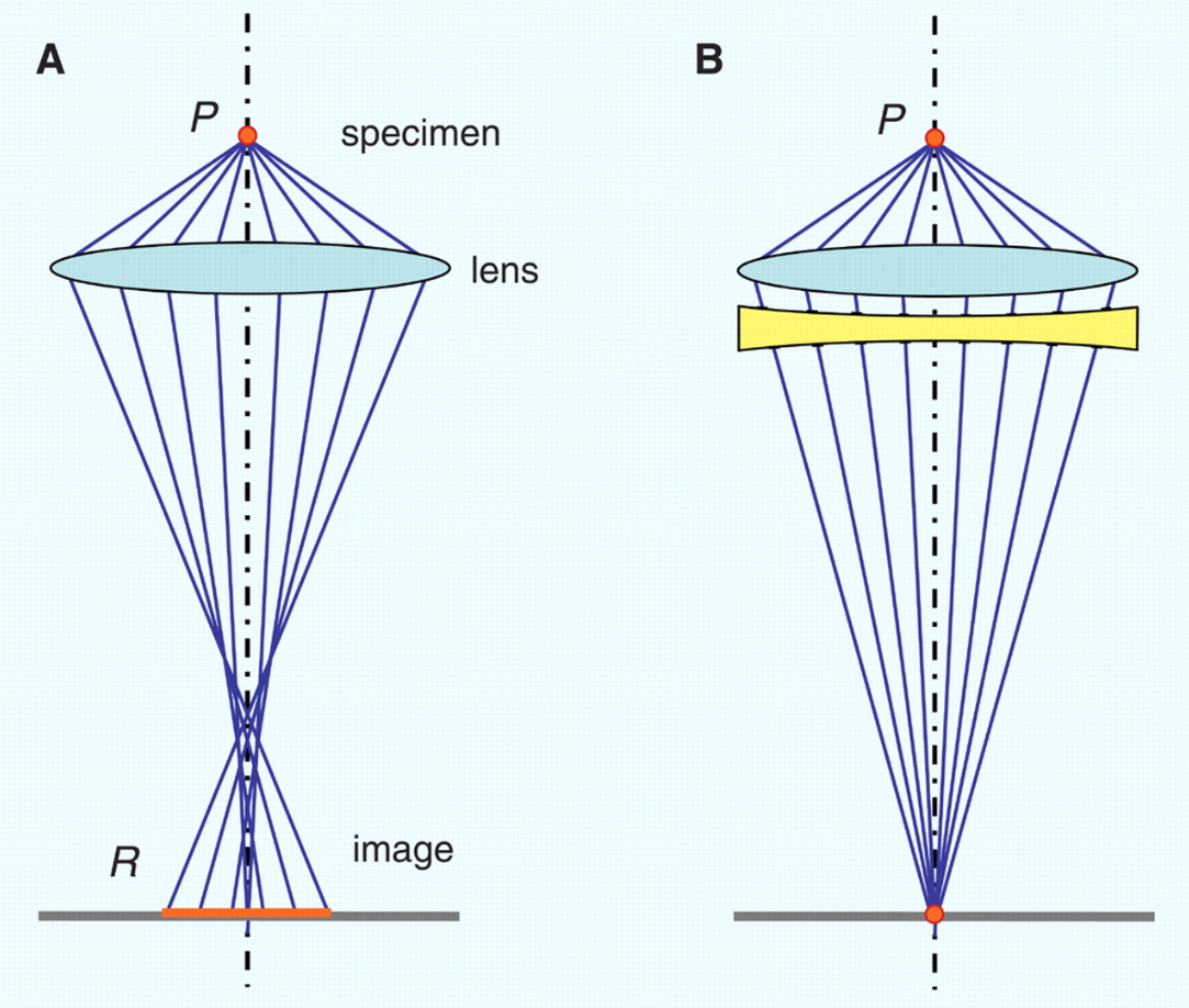
Urban, K. W. Science. 2008.
Figure 1. (A) Schematic Illustration of Spherical Aberration of a Converging Lens. (B) Spherical Aberration is Compensated by Combining the Converging Lens with a Suitable Diverging Lens.
Service at MtoZ Biolabs
MtoZ Biolabs offers comprehensive Aberration Corrected Scanning Transmission Electron Microscopy (AC-STEM) Analytical Services, enabling researchers to visualize atomic structures and compositional variations with unmatched precision. Utilizing advanced AC-STEM platforms, our service supports high-resolution STEM-HAADF imaging for direct observation of atomic column arrangements and Z-contrast visualization. Simultaneously, we provide nanoscale elemental mapping through Energy-Dispersive X-ray Spectroscopy (EDS), revealing detailed distribution of constituent elements within targeted regions. For deeper insight into chemical bonding and electronic structure, our EELS (Electron Energy Loss Spectroscopy) mapping capabilities allow us to identify oxidation states, detect light elements, and characterize fine electronic transitions. Through the integration of these techniques, MtoZ Biolabs delivers rich, correlative datasets capturing atomic arrangements, microstructural features, and elemental distributions, supporting advanced material characterization across diverse scientific disciplines.
Service Advantages
1. Customizable Analytical Protocols
Flexible analytical workflows are tailored to specific research questions, whether probing grain boundary chemistry, interface sharpness, or dopant distribution.
2. Expert Interpretation and Custom Reporting
Our experienced analysts deliver high-quality imaging, validated spectral data, and clear, publication-ready reports tailored to your research goals.
3. One-Time-Charge
Our pricing is transparent, no hidden fees or additional costs.
Applications
Aberration Corrected Scanning Transmission Electron Microscopy (AC-STEM) Analytical Service enables a wide range of high-impact applications across multiple industries:
1. Materials Science: Atomic-level analysis of grain boundaries, dislocations, stacking faults, and phase interfaces in alloys and ceramics.
2. Semiconductor Industry: Characterization of gate oxides, transistor channels, dopant distributions, and failure sites in integrated circuits.
3. Nanotechnology and Catalysis: Visualizing active sites on nanoparticles, atomic dispersion of dopants, and interfacial strain in catalytic systems.
4. Energy Materials: Mapping of lithium distribution in battery electrodes, analysis of perovskites and fuel cell membranes.
5. Thin Films and Coatings: Examination of interface structure, layer uniformity, and diffusion phenomena in multilayer films.
6. Quantum and Photonic Materials: Investigation of atomic ordering, defect states, and heterostructures in 2D materials and quantum dots.
Case Study
Atomic-Scale Visualization of Single-Atom Catalysts for Electrocatalytic Urea Synthesis
In this study, researchers developed a copper single-atom catalyst supported on CeO₂ (Cu₁–CeO₂) for efficient electrocatalytic urea synthesis via C–N coupling between CO₂ and nitrate. Using aberration-corrected HAADF-STEM imaging, they confirmed the atomic dispersion of Cu atoms and resolved the CeO₂ lattice fringes at sub-nanometer resolution. Elemental mapping via EDS further validated the uniform distribution of Cu, Ce, and O across the nanorod framework. This work demonstrates how AC-STEM, combined with EDS, enables direct visualization of single-atom configurations and compositional uniformity, providing critical structural insights into catalyst design and active site identification.
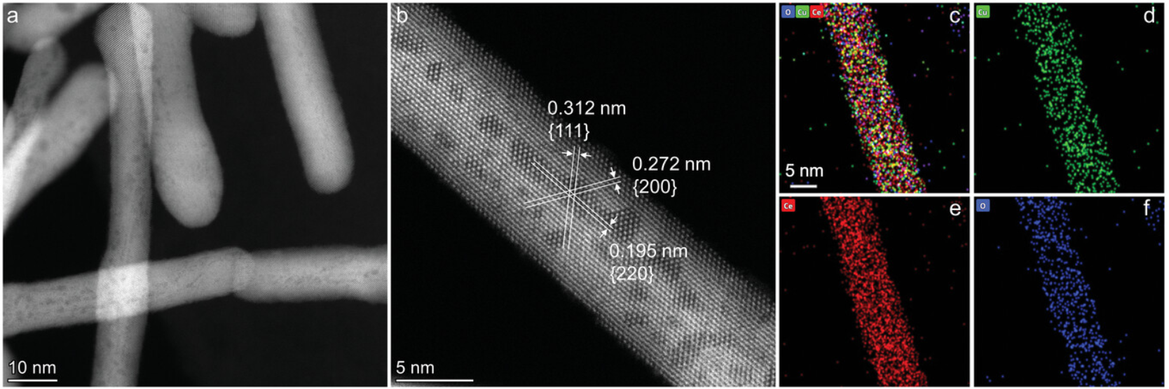
Figure 2. (a) Aberration‐Corrected Transmission Electron Microscopy (AC‐TEM) Image.
(b) Aberration‐Corrected High‐Angle Annular Dark‐Field Scanning Transmission Electron Microscopy (HAADF‐STEM) Image of L‐Cu₁-CeO₂.
(c–f) Elemental Mappings of Copper, Cerium, and Oxygen of L‐Cu₁-CeO₂.
FAQ
Q: What types of information can AC-STEM provide?
AC-STEM enables atomic-resolution imaging and compositional analysis. It provides direct visualization of atomic arrangements (via STEM-HAADF), elemental distribution (via EDS mapping), and electronic structure or bonding states (via EELS mapping).
Free project evaluation, welcome to learn more details! Our technical specialists are available to provide a free business assessment.
How to order?